Choosing a PCB partner is rarely just a search for the lowest quoted price. A dependable supplier must turn design files into boards that fit, function, and arrive when production needs them. This guide explores top PCB manufacturing and assembly companies worldwide, with attention to capabilities buyers can verify: prototype support, production scale, component sourcing, quality controls, and delivery options.
The phrase pcb manufacturing and assembly covers connected but distinct services. A factory may excel at multilayer fabrication yet offer limited assembly capacity. Another may handle surface-mount placement, inspection, and testing under one roof. Details matter. Ask whether the provider supports your board thickness, copper weight, component package, and expected volume. A sample board, inspection report, or clearly documented engineering review can reveal more than a polished sales page.
Global reach can help with capacity and logistics, but it does not guarantee an easy project. Communication delays, changing component availability, and shipping time can affect schedules. Even experienced buyers sometimes miss small process differences. That is worth admitting. Company rankings also depend on the project: a rapid prototype order needs different strengths from a long production run. The sections ahead compare providers through practical criteria rather than treating one name as the universal best. Use the overview to shape questions, verify current capabilities directly, and match each supplier’s strengths to your design, budget, and timeline.

PCB manufacturing and assembly companies convert circuit designs into boards that can perform reliably inside real products. Manufacturing begins with laminate selection, copper patterning, drilling, plating, and solder-mask application. Each step affects electrical performance and physical fit. A misplaced via or rough hole can disrupt a signal or weaken a connection.
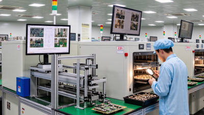
Assembly teams then apply solder paste, place components, and heat the board in a controlled reflow oven. They may add hand-soldering, inspection, and functional testing for connectors, power circuits, or sensitive components.
Prismark’s 2024 PCB industry report estimated global PCB production value at about $68.4 billion in 2023, down roughly 15% from 2022. That contraction underscores how demand shifts can affect capacity and lead times. Small details matter.
The work also includes design-for-manufacturing feedback. Engineers may flag narrow spacing, awkward panel layouts, or components that are difficult to source before production begins. Automated optical inspection checks visible solder and placement issues; electrical tests look for open or short circuits.
Still, inspection cannot fix every design weakness. A tidy test result does not guarantee that a board will tolerate heat, vibration, or years of use. The handoff between design, fabrication, and assembly can be imperfect, so clear drawings and documented test limits are essential.
PCB production begins with a design review that checks stack-up, trace width, spacing, and drill sizes. This can catch fabrication problems before panels reach the production line. Material selection matters. Copper weight, laminate thickness, and temperature ratings influence signal behavior and board reliability. Yet a specification may not capture every condition the finished board will face.
During fabrication, imaging transfers circuit patterns onto copper-clad panels, followed by etching and drilling. Plating forms conductive walls inside through-holes, while solder mask protects copper between pads. Layer registration needs careful control, since small shifts can weaken fine-pitch connections. Automated optical inspection helps find shorts, opens, and pattern defects, though it cannot explain every cause.
Assembly adds another layer of process control. Stencil printing, component placement, and reflow soldering must work together; paste volume and thermal profiles deserve close attention. Capable manufacturers may support prototypes, production runs, traceability, and electrical testing suited to the board’s intended use. Functional tests can reveal issues that visual checks miss. Test coverage has limits.
| Production stage | Capability dimension | Typical commercial range | Key considerations |
|---|---|---|---|
| Board types | Rigid, flexible, and rigid-flex circuit boards | Rigid boards are widely produced; flex and rigid-flex designs require specialized materials and processing | Material selection, bend requirements, board outline, and application determine manufacturability. |
| Layer construction | Number of copper layers | 2–20 layers are common commercial configurations; higher layer counts are available for specialized designs | Stack-up symmetry, impedance targets, thermal performance, and registration tolerances affect yield. |
| Circuit imaging | Minimum trace width and spacing | Approximately 75–150 µm for many conventional designs; 40–75 µm for HDI; finer geometries require specialized processes | Copper weight, panel size, layer count, and etching capability influence achievable geometry. |
| Drilling and interconnects | Mechanical holes and laser-drilled microvias | Mechanical drill diameters around 0.15–0.30 mm are common; laser microvias are often around 0.075–0.15 mm | Via structure, aspect ratio, plating, and reliability requirements should be confirmed during design review. |
| Lamination and stack-up | Board thickness and plated-hole aspect ratio | Approximately 0.4–3.2 mm covers many standard board designs; 8:1 is a common design target for plated through-holes | Thicker boards and higher aspect ratios may require additional process controls and qualification. |
| Surface finishing | Solderable finishes | Common options include lead-free HASL, ENIG, immersion silver, immersion tin, and OSP | Finish choice depends on shelf life, soldering process, contact requirements, and environmental specifications. |
| Component assembly | SMT package and pitch capability | 0201 imperial passive components and BGA pitches around 0.4–0.8 mm are common in capable SMT production; finer pitches are specialized | Component availability, stencil design, board warpage, and placement accuracy affect assembly results. |
| Inspection and test | Manufacturing and assembly verification | Common methods include AOI, X-ray inspection, flying-probe or fixture-based electrical test, and functional test | Test coverage should be matched to product risk, design access, acceptance criteria, and production volume. |
| Quality requirements | Industry standards and acceptance criteria | Relevant standards may include IPC-6012 or IPC-6013 for bare boards, and IPC-A-610 or J-STD-001 for assembly | The required class, documentation, traceability, and inspection plan should be specified for each project. |
Capability ranges are indicative industry examples, not guarantees; actual limits vary by facility, materials, design rules, and qualification requirements.
A capable PCB manufacturing and assembly provider should fit your board’s requirements, not just offer an attractive price. Start with the basics: board dimensions, layer count, copper weight, materials, and expected production volume.
Ask whether the provider can explain its design-for-manufacturing checks before fabrication begins. Request sample inspection reports and ask how it tracks materials and production batches. Details matter.
For assembly, check component sourcing controls, placement accuracy, soldering methods, and inspection options such as automated optical inspection or X-ray inspection. A polished sales response is not proof of consistent process control.
Evaluate communication as carefully as equipment. Ask who reviews engineering questions, how changes are documented, and when you will receive production updates. A clear quote should identify tooling, testing, shipping, and any assumptions that could affect cost or schedule.
If possible, compare a prototype run with the provider’s stated process, then review defects and corrective actions—not only whether the boards passed.
A low quote can still be useful, but only when its scope is clear. It is easy to overvalue certifications or machine lists; neither shows how a supplier handles a real build. Ask for evidence, and leave room for a second opinion when the technical answers feel vague.
Leading PCB manufacturing and assembly companies worldwide are evaluated by more than factory size or quoted price. A dependable partner can translate a schematic into a practical stack-up, flag tight clearances, and explain how material choices affect signal integrity and cost. Ask for capability data covering layer count, copper weight, minimum drill size, and controlled impedance. Details matter. A polished capability sheet is useful, but recent production examples and clear engineering responses offer stronger evidence.
Assembly capability deserves equal attention. Check whether the supplier manages component sourcing, stencil design, surface-mount placement, reflow profiling, and inspection within a documented process. Ask how it handles solder-paste checks, X-ray review for hidden joints, electrical testing, and lot traceability. Not every board needs every test. The right plan depends on design risk, volume, and operating conditions. Worldwide providers may offer useful regional coverage, yet shipping time, communication overlap, and change-control discipline can vary. Request a pilot build with agreed acceptance criteria before scaling. Even then, no checklist removes all risk; a missed assumption can survive review, so keep design and production teams talking.
Worldwide printed circuit board market, USD billions
The chart shows reported market estimates, not the revenue or ranking of individual manufacturers or assembly providers. The market was valued at $76.1 billion in 2023 and is forecast to reach $120.2 billion by 2032. Source: Fortune Business Insights, Printed Circuit Board Market report.
Regional markets shape the global PCB industry in different ways. Asia remains the main production center, supported by dense supplier networks across China, Japan, South Korea, and Taiwan. These markets serve high-volume consumer electronics while investing in advanced packaging substrates and high-density interconnect boards. North America and Europe tend to emphasize automotive, industrial, medical, and aerospace applications, where traceability and specialized engineering matter. The picture is not tidy: regional capacity and local sourcing are changing, but skilled labor and material access remain uneven. Prismark estimated global PCB production value at about $73.6 billion in 2024, a 5.8% year-over-year increase. Its industry outlook also highlights demand from AI servers, automotive electronics, and advanced substrates as growth drivers.
Tips: Compare suppliers by process capability, not location alone. Ask about layer count, via structures, trace spacing, assembly capacity, and delivery performance. A factory’s address does not prove its reliability. Request recent, relevant quality data before making a decision.