What is Printed Circuit Board Design and its Importance in Electronics?
Printed circuit board design is a fundamental aspect of modern electronics. It serves as the backbone for nearly all devices we use today. From smartphones to complex industrial machines, the effectiveness of these devices hinges on their PCB designs. Engineers face numerous challenges in this field, requiring both creativity and technical skill.
The importance of printed circuit board design cannot be overstated. A well-designed PCB ensures not only the functionality but also the reliability of the final product. Precision in layout and material selection can prevent failures in the field. However, designers often overlook potential issues like thermal management and signal integrity. These factors, if neglected, can lead to significant performance problems.
Moreover, as technology evolves, so do the demands of PCB design. Designers must stay updated with trends such as miniaturization and integration. This constant change can lead to stress and the risk of mistakes. Embracing a mindset of continuous improvement is crucial. The journey of mastering printed circuit board design is ongoing, with both successes and setbacks along the way.
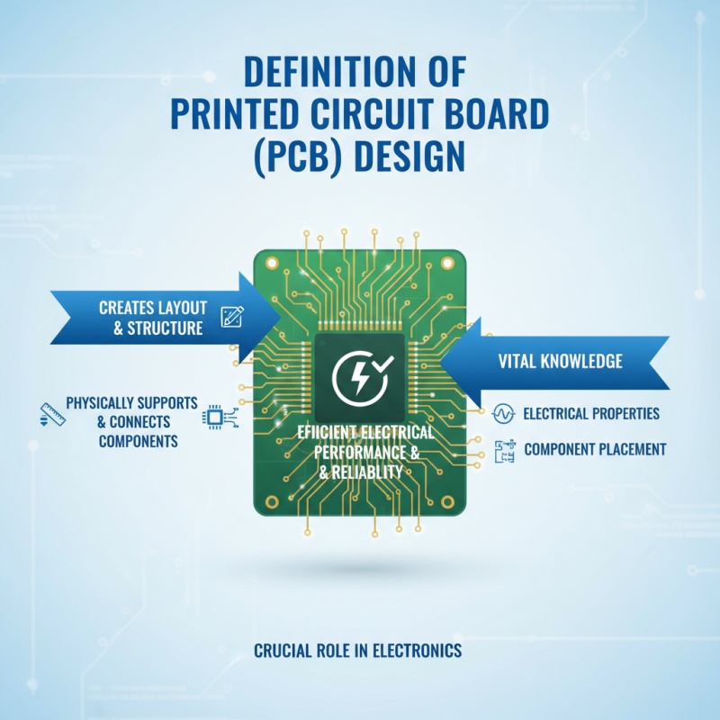
Definition of Printed Circuit Board (PCB) Design
Printed Circuit Board (PCB) design plays a crucial role in electronics. It refers to the process of creating the layout and structure of a PCB, which physically supports and connects electronic components. A well-designed PCB ensures efficient electrical performance and reliability. Knowledge about electrical properties and component placement is vital in this process.
Creating a PCB involves using specialized software. Designers must carefully consider traces, vias, and pads to ensure a functional circuit. Mistakes in design can lead to circuit failures, causing frustration and financial loss. Verification steps should not be overlooked. They guarantee that the design adheres to required specifications.
**Tip:** Always double-check your connections. Small errors can lead to significant problems.
Moreover, understanding manufacturing constraints is critical. Different materials and methods affect the final product's quality and performance. Designers should learn about the latest technologies, like flexible PCBs. Keeping pace with advancements is essential in this rapidly evolving field.
**Tip:** Regularly update your design skills. It can save time and enhance your work quality.
Key Components of PCB Design and Their Functions
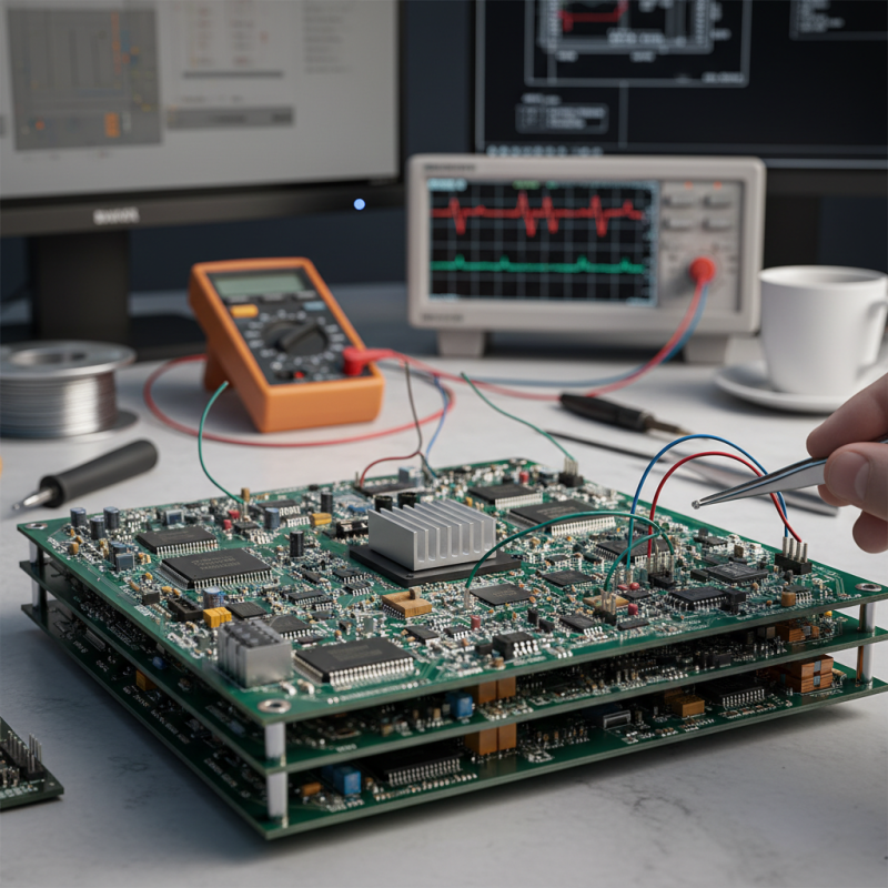
Printed Circuit Board (PCB) design is critical in electronics. It involves several key components, each serving a specific function. The primary elements include traces, pads, and vias. Traces connect different components, allowing electrical signals to flow. Pads serve as landing areas for components like resistors, capacitors, and integrated circuits. Vias link different layers of a multi-layer PCB, enhancing connectivity.
According to a 2023 report by PCB Design Trends, an estimated 70% of electronic device failures arise from poor PCB design. This highlights the significance of precision in designing traces and placing pads. Mistakes can lead to signal integrity issues or thermal problems. Inspecting the layout and ensuring the correct size for pads is essential. Design complexity often leads to overlooked details, which could prove detrimental.
Additionally, simulation tools are now fundamental in PCB design. They help engineers foresee potential design flaws before manufacturing. However, these tools also require a learning curve. Some engineers may not fully utilize their capabilities. This underlines the need for continuous education in PCB design best practices. Incorporating emerging technologies can provide substantial improvements. Yet, engineers must balance innovation with reliability.
The PCB Design Process: Steps and Best Practices
Designing a printed circuit board (PCB) requires a structured approach. The process begins with defining the functional specifications. Knowing what the PCB should achieve is crucial. Engineers must gather requirements like size, component types, and power needs. This phase can be challenging. Miscommunications can lead to significant redesigns later.
Next comes creating the schematic design. This is the blueprint for the entire circuit. It includes all components and their connections. During this stage, attention to detail is vital. A small mistake can result in a malfunctioning board. Reviewing and revising the schematic is a common practice. Many professionals advocate for a second set of eyes during this phase.
The layout process follows. Here, engineers position components on the board. Routing the electrical connections accurately is critical. This step can be tedious, and adjustments may be needed. Designers often find it necessary to go back and forth. Each revision helps perfect the compactness and functionality of the PCB. Balancing performance with manufacturability requires experience and insight.
Importance of PCB Design in Modern Electronics
Printed Circuit Board (PCB) design plays a critical role in modern electronics. It serves as the backbone of virtually all electronic devices. Proper PCB design ensures the efficient functioning of components by managing the electrical pathways effectively. An optimized design improves performance while reducing signal interference. Engineers must consider various factors, such as component placement, trace routing, and grounding.
Moreover, the complexity of today's electronics demands high precision in PCB design. Designers often use advanced software tools to create intricate layouts. However, mistakes can occur, leading to costly revisions. For example, rushed designs might overlook thermal management, causing overheating issues. Furthermore, inadequate spacing between traces can lead to signal integrity problems.
In an era where technology evolves rapidly, PCB design becomes even more essential. It directly affects the durability and functionality of devices. Designers must continuously learn and adapt to new materials and techniques. Despite advancements, the importance of foundational knowledge remains clear. Emphasizing attention to detail and thorough testing is crucial for successful PCB design.
Challenges and Innovations in PCB Design Techniques
In the ever-evolving field of electronics, PCB design plays a crucial role. However, this process is not without its complexities. Designers often face challenges like minimizing electromagnetic interference and ensuring thermal management. These issues demand innovative solutions to maintain performance and efficiency in modern devices.
Recent advancements in PCB design techniques offer promising solutions. For instance, the use of advanced simulation tools helps predict and resolve issues before production begins. Designers can visualize potential failures in a virtual space, reducing costly errors. Additionally, materials like flexible PCBs are gaining popularity, enabling more compact and lightweight designs. However, adapting to new technologies often requires a steep learning curve.
Despite these innovations, there are still gaps to address. Not every designer is equipped with the latest tools, leading to inconsistencies in quality. Embracing new methodologies can enhance the design process, but training and resources remain essential. Designers must continually seek knowledge and share experiences to overcome these hurdles and drive the industry forward.
What is Printed Circuit Board Design and its Importance in Electronics?
| Dimension |
Description |
| Layer Count |
The number of conductive layers in a PCB, affecting complexity and functionality. |
| Material Type |
Common materials include FR-4, CEM-1, or Rogers for high-frequency applications. |
| PCB Thickness |
Typical thickness ranges from 0.2 mm to 3.2 mm, influencing strength and durability. |
| Trace Width |
Width of the conductive pathways; critical for current capacity and resistance. |
| Impacts of Design |
Influences manufacturability, performance, and reliability of electronic devices. |
| Design Software |
Tools like Altium Designer, Eagle, or KiCAD to aid in PCB design and layout. |