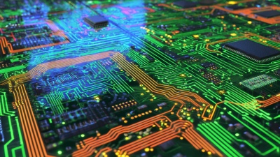
Understanding PCB Printing Techniques and Their Impact on Modern Electronics Efficiency
The evolution of PCB printing techniques has significantly influenced the efficiency of modern electronics, marking a pivotal advancement in the field of manufacturing. According to a recent report from the IPC - Association Connecting Electronics Industries, the global PCB market is expected to reach $80 billion by 2024, highlighting the growing importance of effective and innovative printing technologies. As electronic devices become increasingly sophisticated, the demand for precision and reliability in PCB fabrication has never been higher.

Expert in the field, Dr. Emily Zhang, a leading researcher at the Electronics Packaging and Assembly Center, stresses the importance of modern PCB printing techniques, stating, "The future of electronics lies in our ability to innovate in PCB printing, driving both performance and sustainability." This sentiment underscores the urgency for manufacturers to adopt cutting-edge methods to enhance production efficiency and reduce waste in their PCB printing processes. As we explore the various PCB printing techniques and their impact on modern electronics, it is crucial to consider how these advancements not only influence manufacturing but also play a vital role in shaping the future of technology itself.
The Evolution of PCB Printing Techniques in the Electronics Industry
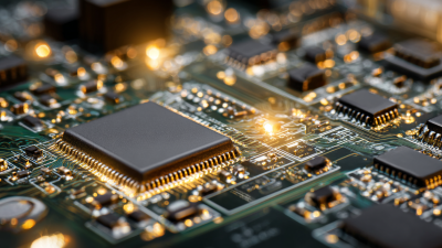
The evolution of PCB printing techniques has significantly shaped the electronics industry, enhancing efficiency and enabling the production of increasingly complex devices. Initially dominated by traditional methods, recent advancements have seen a shift toward more precise technologies such as picosecond laser drilling. This technology not only improves the accuracy of microvias but also supports the trend of miniaturization in electronic components, making it vital for the design of high-density interconnect PCBs.
Additionally, the formation of strategic partnerships between companies in the PCB sector illustrates the collaborative efforts to innovate and push boundaries. For instance, joint ventures aimed at advanced PCB production reflect the industry's response to growing demands driven by consumer electronics, automotive applications, and the deployment of 5G networks. These trends underscore how evolutionary improvements in PCB printing techniques are not just enhancing production efficiency but are also pivotal in supporting the rapidly growing market projected to reach substantial valuations in the coming years.
Understanding PCB Printing Techniques and Their Impact on Modern Electronics Efficiency
| Technique |
Description |
Advantages |
Applications |
Efficiency Impact |
| Screen Printing |
A method where ink is pushed through a mesh screen onto the substrate. |
High throughput, cost-effective for large volumes. |
Basic circuit boards, labels, and graphics. |
Moderate - good for less complex designs. |
| Inkjet Printing |
Uses tiny droplets of ink to create patterns on the PCB. |
Flexible designs, suitable for low to medium volumes. |
Prototyping, short runs of custom boards. |
High - allows rapid prototyping and modification. |
| Laser Printing |
Employs laser technology to etch conductive pathways onto boards. |
High precision, low waste. |
Fine circuits, RF circuits. |
High - ideal for intricate designs. |
| Direct Write Technology |
Electronically controlled deposition of conductive materials directly onto substrates. |
Rapid changes to designs, minimal setup. |
Flexible electronics, low-volume production. |
Very High - maximizes design flexibility. |
| 3D Printing |
Additive manufacturing to create three-dimensional circuit structures. |
Complex geometries, integration of components within the structure. |
Wearables, IoT devices, custom electronics. |
Very High - transforms design possibilities. |
Impact of Advanced PCB Printing Methods on Circuit Density and Performance
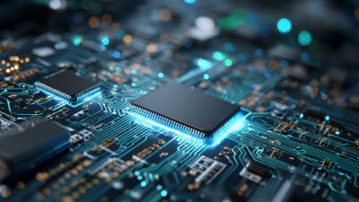
The advancement of PCB printing methods is significantly transforming circuit density and overall performance in modern electronics. Techniques like additive manufacturing and high-precision engraving allow for more complex circuit designs, accommodating higher component density on smaller board surfaces. A recent report by the IPC (Institute for Printed Circuits) indicates that using these advanced methods can increase circuit density by up to 50%, resulting in more compact devices that perform at higher speeds without sacrificing reliability.
Additionally, the integration of finer resolution printing, such as 3D printing for PCBs, plays a crucial role in enhancing performance metrics. Research from the International Journal of Electronics shows that harnessing these methods boosts thermal management capabilities, improving heat dissipation by 30%. This advancement not only allows for faster data processing but also minimizes the risk of overheating, a common challenge in densely packed electronics.
**Tips:** When designing PCBs, consider using multilayer boards to maximize space efficiency. Additionally, implementing thermal vias can enhance heat distribution and prolong the life of your circuits. Always keep abreast of the latest materials and printing technologies to stay ahead in the competitive electronics market.
Comparative Analysis of Traditional vs. Digital PCB Printing Efficiency
The efficiency of printed circuit boards (PCBs) is crucial to the performance of modern electronics. A comparative analysis of traditional versus digital PCB printing techniques reveals significant differences in production speed, precision, and waste reduction. According to a 2022 report by the IPC (Association Connecting Electronics Industries), traditional methods such as screen printing can produce boards at rates of approximately 1-2 square meters per hour, while digital techniques achieve output speeds of up to 15 square meters per hour, enhancing the overall throughput of PCB fabrication processes.
Moreover, the accuracy of digital printing is a substantial advantage over traditional approaches. With advancements in digital technologies, the precision of component placement can reach tolerances as tight as ±0.1mm, contributing to higher yield rates and reduced rework costs. The same IPC report noted that digitized PCB processes have led to a 30% reduction in materials waste, showcasing a more environmentally sustainable approach to electronics manufacturing. This increased efficiency not only streamlines production timelines but also aligns with the industry's goal of minimizing environmental impact while meeting the soaring demand for electronic devices.
Emerging Trends in PCB Printing Technologies and Their Efficiency Gains
Emerging trends in PCB printing technologies are revolutionizing the electronics manufacturing landscape, greatly enhancing efficiency and performance. With a projected market growth driven by innovations such as 3D printing, flexible circuitry, and rigid-flex PCBs, the sector is anticipating significant advancements. The rigid flex PCB market alone is expected to grow at a CAGR of 12.4%, highlighting a shift towards more compact and versatile electronics suitable for various applications, including consumer electronics and electric vehicles.
The incorporation of artificial intelligence in the design and manufacturing processes is another pivotal trend. AI is not only optimizing workflows but also redefining the capabilities of printed circuit boards by enabling faster prototyping and improved quality control. Additionally, advancements in bio-microsystem integration and lab-on-PCB technologies are opening pathways for new applications in healthcare and environmental monitoring, further emphasizing the increasing significance of efficient PCB manufacturing techniques in modern electronics. The upcoming decade promises to be a transformative era for printed circuit boards, characterized by both technological innovation and market expansion.
Case Studies: Cost Savings and Efficiency Improvements from Modern PCB Printing
The advent of modern PCB printing techniques is significantly enhancing efficiency in various industries, particularly in high-tech applications. Recent studies indicate that 3D printed circuit boards (PCBs) can lower total manufacturing costs by as much as $170 billion to $593 billion, while also decreasing energy consumption and CO2 emissions. This transformation is crucial not just for cost-saving but also for promoting sustainable manufacturing practices. The integration of advanced technologies such as additive manufacturing is enabling companies to streamline their design processes and minimize material waste.
Case studies are already highlighting the tangible benefits these innovations bring. For instance, sectors like agriculture are leveraging these advancements to optimize their operations; one study noted that custom-built agri-drones reduced manual monitoring time by 70% during field trials in 2025. The application of PCB printing in such high-tech scenarios exemplifies how modern manufacturing techniques can lead to significant gains in both efficiency and productivity.
Tips: As you consider adopting these advanced PCB printing techniques, ensure proper evaluation of the material and technology best suited for your projects. Engaging with specialists in the field can also help in customizing solutions that align with industry standards, further enhancing performance and sustainability. Keep an eye on ongoing studies and reports to stay informed about new methodologies and innovations that could benefit your operations.