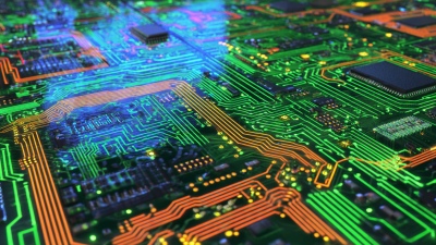
10 Essential PCB Printing Techniques You Need to Know
In the rapidly evolving world of electronics, the significance of PCB printing cannot be overstated. As reported by the IPC Association Connecting Electronics Industries, the global printed circuit board (PCB) market is projected to reach $83 billion by 2024, driven by innovations in technology and a surge in demand from various sectors including automotive, telecommunications, and consumer electronics. With such rapid growth, understanding the essential PCB printing techniques is crucial for manufacturers aiming to remain competitive. The right printing methods can enhance efficiency, reduce costs, and improve product quality, making them integral to the production process.
As we explore the essential PCB printing techniques, we will also consider alternative types that can further optimize performance and sustainability in PCB design and fabrication.
Understanding the Basics of PCB Printing Techniques
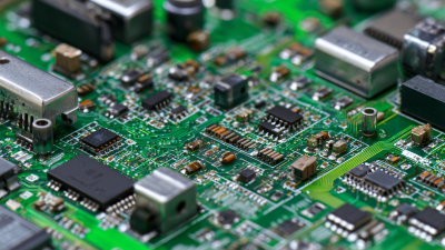
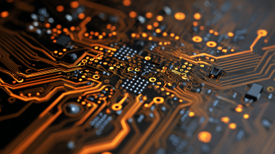
Printed Circuit Boards (PCBs) form the backbone of modern electronic devices, and understanding the basics of PCB printing techniques is crucial for engineers and hobbyists alike. The printing process involves transferring circuit designs onto a substrate material, typically ensuring that electrical connections are created in a reliable and efficient manner. At its core, the process can include various methods such as screen printing, inkjet printing, and direct imaging, each offering unique advantages and processes suited for different applications.

Screen printing remains one of the most common techniques due to its versatility and cost-effectiveness. It involves using a mesh screen to apply conductive ink directly onto the board's surface, perfect for large runs and thicker applications. In contrast, inkjet printing has gained popularity for its ability to produce intricate designs with high precision, particularly useful in multi-layer PCBs where space is at a premium. Additionally, direct imaging technology allows for rapid prototyping, reducing the time from design to production, thus catering to the fast-paced nature of electronic development. Understanding these fundamental techniques empowers creators to choose the right method tailored to their specific needs, paving the way for innovation in PCB design.
Exploring the Advantages of Screen Printing in PCB Production
Screen printing is a widely favored method in PCB production, primarily due to its capability to create highly detailed and precise designs. This technique allows for the application of thick layers of solder paste and conductive inks, which are crucial for ensuring strong electrical connections.
One significant advantage of screen printing is its ability to handle various substrates and materials, making it versatile for different types of circuit boards.
Another important benefit of screen printing in PCB manufacturing is its efficiency in mass production. The process can be automated, significantly reducing the time taken to apply ink or solder paste across multiple boards. This high throughput ensures that large quantities of PCBs can be produced rapidly without compromising on quality. Additionally, screen printing is cost-effective, as it minimizes waste and maximizes material usage, making it an ideal choice for manufacturers looking to optimize their production processes. Overall, the advantages offered by screen printing make it an essential technique for anyone involved in PCB production.
The Role of Photoengraving in High-Precision PCBs
Photoengraving plays a pivotal role in the production of high-precision printed circuit boards (PCBs). This technique allows for the transfer of intricate circuit designs onto PCB substrates, achieving resolutions as fine as 10 microns. According to a report by IPC, nearly 90% of PCB manufacturers recognize photoengraving as essential for ensuring production accuracy and quality. This precision is critical in industries such as aerospace and medical devices, where even the slightest error can lead to significant failures.
When utilizing photoengraving for PCB production, it's crucial to maintain optimal exposure settings to guarantee the best results. A tip for manufacturers is to regularly calibrate exposure units and use quality films for photomasks, as this can directly impact the fidelity of the final product. Additionally, keeping the workspace free of dust and contaminants can dramatically improve the quality of the engravings.
Furthermore, adopting a rigorous testing protocol post-engraving can ensure that defects are identified early before proceeding to subsequent manufacturing stages. Utilizing equipment that tests for copper thickness and etch ratios helps to maintain the integrity of the PCB design. By implementing these strategies, manufacturers can leverage photoengraving to produce highly reliable and precise PCBs that meet the growing demands of modern electronic applications.

How to Choose Between Inkjet and Laser Printing for PCB Design
When it comes to PCB design, selecting the right printing technique is crucial for ensuring precision and quality. Two of the most popular options—inkjet and laser printing—both offer distinct advantages and disadvantages that can influence your final choice. Inkjet printing is renowned for its ability to produce high-resolution images and intricate designs, making it ideal for prototypes and small-batch productions. Its versatility allows for printing directly onto various substrates, which is beneficial when working with specialized materials.
On the other hand, laser printing is often favored for its speed and efficiency in large production runs. Laser printers can handle thicker materials and provide excellent adhesion, making them suitable for long-lasting printed circuit boards. However, they may lack the fine detail that inkjet printers can achieve. Ultimately, the decision between inkjet and laser printing for PCB design should be guided by your project requirements, including the complexity of the design, the production volume, and the specific properties you need in the final product.
10 Essential PCB Printing Techniques You Need to Know
| Technique |
Description |
Ideal Uses |
Pros |
Cons |
| Inkjet Printing |
Uses liquid inks to produce images and designs on PCB. |
Prototyping, low-volume production. |
Low setup costs, flexibility. |
Less durable, slower speeds. |
| Laser Printing |
Uses laser technology to transfer toner onto PCB. |
High-volume production, high precision needs. |
High speed, durable results. |
Higher setup costs, less material flexibility. |
| Screen Printing |
Uses a mesh screen to transfer ink onto the PCB. |
Large runs, thicker inks. |
Cost-effective for large volumes. |
Not suitable for fine detail. |
| UV Printing |
Uses ultraviolet light to cure ink as it is printed. |
Custom designs, vibrant colors. |
Quick drying, high impact visuals. |
Higher equipment costs, limited materials. |
| Conductive Ink Printing |
Uses conductive inks to create electrical circuits. |
Wearable electronics, sensors. |
Flexibility, lightweight designs. |
Limited conductivity, requires careful handling. |
Essential Tips for Optimizing Your PCB Printing Process
Optimizing your PCB printing process is crucial for enhancing efficiency and minimizing costs. One key aspect is the selection of appropriate materials. According to a recent study by IDTechEx, nearly 40% of the operational costs in PCB manufacturing can be attributed to material waste. By employing high-quality inks and substrates that are specifically engineered for your application, manufacturers can significantly reduce waste and improve print fidelity. Utilizing advanced inkjet technology not only improves the precision of the designs but also allows for rapid prototyping, reducing the lead time drastically.
Another essential consideration is the calibration of printing equipment. The IPC (Institute of Printed Circuits) reports that proper calibration can increase print quality by up to 25%, directly impacting the overall integrity of the PCB. Implementing rigorous quality checks throughout the printing process, including environmental controls for temperature and humidity, can help maintain consistent results. Additionally, regularly updating software and firmware of printing machines ensures they function optimally, thus preventing costly downtimes and reprints. By focusing on these optimization tips, manufacturers can achieve a more streamlined and cost-effective PCB printing process.