Emerging Trends in Circuit Board Design for 2025: Innovating for the Future
As we look toward 2025, the landscape of circuit board design is set to undergo significant transformations driven by technological advancements and market demands. The global printed circuit board (PCB) market is expected to reach approximately $83.5 billion by 2025, reflecting a compound annual growth rate (CAGR) of around 3.4% from 2020 to 2025, according to a report by MarketsandMarkets. This growth is largely fueled by the rising need for miniaturization in electronics, increased adoption of IoT devices, and the push towards sustainable manufacturing practices. However, as innovations emerge, challenges persist, including the complexity of designs, thermal management issues, and the integration of new materials. To navigate these evolving dynamics, it is essential to examine industry case studies that highlight practical applications and address common problems associated with circuit board design, paving the way for future innovations.
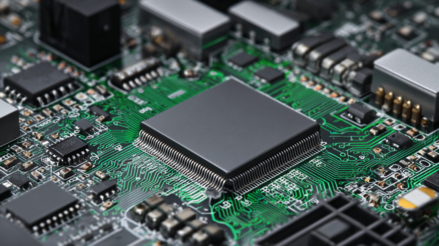
Key Materials Revolutionizing Circuit Board Design in 2025
The landscape of circuit board design is set for a transformative shift as we approach 2025, driven by innovative materials that promise to enhance performance and efficiency across various applications.
 One of the most significant trends is the emergence of high-frequency laminate materials, which are designed to minimize signal loss and maximize thermal performance. These materials, such as Teflon and polyimide composites, enable circuit boards to operate effectively in demanding environments, making them ideal for applications in telecommunications and aerospace.
Another key material revolutionizing circuit board design is the adoption of flexible and stretchable substrates. These materials provide unparalleled versatility, allowing designers to create boards that conform to non-flat surfaces and can withstand mechanical stress without compromising functionality. With the rise of wearable technology and Internet of Things (IoT) devices, the ability to produce lightweight and adaptable circuit boards is becoming increasingly crucial. The integration of conductive inks and organic substrates further enhances the capability of these designs, paving the way for new applications that were once thought impossible.
As these innovations unfold, 2025 promises to be a pivotal year for the evolution of circuit board design, propelling industries toward a more connected and efficient future.
Advanced Manufacturing Techniques for Tomorrow's Circuit Boards
As we look ahead to 2025, the landscape of circuit board design is rapidly evolving. Advanced manufacturing techniques are at the forefront, enabling engineers to create more efficient and complex designs. Techniques such as additive manufacturing and automated assembly are gaining traction, allowing for more intricate structures and reduced material waste. This shift not only enhances performance but also minimizes production costs.
One essential tip for manufacturers is to embrace automation in their assembly processes. By implementing robotic systems, companies can boost productivity and consistently maintain high-quality standards. Furthermore, utilizing simulation software can significantly improve design accuracy and reduce errors during production.
Another critical trend is the integration of sustainable practices into circuit board production. Utilizing eco-friendly materials and energy-efficient processes can not only appeal to environmentally conscious consumers but also meet regulatory standards. Manufacturers should consider investing in green technologies, as they not only contribute to sustainability but can also lead to long-term cost savings.
Sustainability and Eco-Friendly Practices in Circuit Board Innovation
As we look towards 2025, the circuit board design industry is increasingly prioritizing sustainability and eco-friendly practices. The global market for sustainable electronics is projected to grow at a CAGR of 8.5%, reaching approximately $1 trillion by 2025, according to a recent report by MarketsandMarkets. This shift is largely driven by consumer demand for greener products, regulatory pressures, and the need to reduce electronic waste and carbon footprints associated with circuit manufacturing.
Innovations in materials play a crucial role in this transition. Biodegradable substrates, like polylactic acid (PLA) and other bio-based materials, are gaining traction as alternatives to traditional FR4 materials, which are not only more harmful to the environment but also contribute significantly to landfill waste. Furthermore, the adoption of lead-free soldering and water-based coatings is becoming commonplace, minimizing toxic releases during manufacturing processes. A study by the International Electronics Manufacturing Initiative (iNEMI) revealed that implementing these eco-friendly technologies could reduce carbon emissions by up to 30% in the PCB sector by 2025.
Incorporating advanced manufacturing techniques, such as additive manufacturing and smart manufacturing, also enhances sustainability efforts. These methods optimize material usage and reduce waste, aligning with the circular economy principles. Reports indicate that by integrating these innovative practices, the PCB industry stands to save approximately 20% on material costs while simultaneously decreasing environmental impact, showcasing a promising path toward a more sustainable future in circuit board design.
The Role of AI and Automation in Circuit Board Development
As we look towards 2025, the integration of AI and automation in circuit board development is poised to transform the industry dramatically. The use of artificial intelligence allows designers to analyze vast amounts of data quickly, identifying trends and optimizing layouts far more efficiently than conventional methods. For instance, machine learning algorithms can predict potential failure points by examining historical performance data, leading to more resilient designs and reduced prototyping times.
Furthermore, automation plays a crucial role in streamlining the manufacturing process. Robotics and automated systems can handle tasks such as soldering and assembly with precision and speed, ensuring consistent quality while minimizing human error. This shift enables engineers to focus more on creative problem-solving and innovation, rather than being bogged down by repetitive tasks. As we advance, the synergy between AI and automation will not only accelerate production timelines but also enhance the complexity and functionality of circuit designs, driving the next wave of technological advancements.
Emerging Trends in Circuit Board Design for 2025
This chart illustrates the projected advancements in key areas of circuit board design influenced by AI and automation technologies by the year 2025. The data showcases trends in automation adoption, efficiency improvements, and AI integration levels across various sectors.
Future Design Software: Tools Shaping Circuit Board Engineering in 2025
As we look towards 2025, the landscape of circuit board design is evolving rapidly, driven by innovative software tools that enhance engineering processes. One of the most significant trends is the integration of artificial intelligence (AI) in design software. According to a recent report by MarketsandMarkets, the circuit board design software market is expected to reach $2.45 billion by 2025, growing at a CAGR of 8.9%. This growth is largely attributed to the demand for smarter design solutions that reduce time-to-market and improve product reliability.

Moreover, the advent of cloud-based design platforms is reshaping how engineers collaborate on circuit board projects. A study conducted by TechNavio indicates that cloud-based solutions will account for over 30% of the overall circuit design software market by 2025. These platforms not only facilitate real-time collaboration among distributed teams but also offer scalable resources that adapt to the complexity of various projects. With such advancements, designers are empowered to create more intricate and efficient circuit board layouts, paving the way for innovations in various industries, from consumer electronics to aerospace.