5 Best Strategies for Optimizing PCB Manufacturing Assembly Efficiency
In the fast-paced electronics industry, optimizing PCB manufacturing assembly is crucial for maintaining competitive advantage and meeting growing market demands. According to a recent report by IPC, the global PCB market is projected to reach $77 billion by 2025, with assembly efficiency playing a pivotal role in cost reduction and throughput enhancement. Ineffective assembly processes can lead to increased production times and defects, significantly impacting overall product quality and profitability.
As manufacturers strive to improve production capabilities, implementing effective strategies for optimizing PCB manufacturing assembly becomes essential. This blog will explore five best practices that can help streamline processes, reduce waste, and ensure timely delivery of high-quality electronic products in an increasingly competitive landscape.
Understanding PCB Manufacturing: Key Industry Statistics and Trends
The trend of miniaturization in the electronics industry is significantly enhancing the efficiency and reliability of PCB manufacturing. With an increasing demand for smaller, more powerful, and feature-rich devices, the PCB design landscape is evolving rapidly. According to industry reports, the China PCB equipment sector is projected to grow alongside these trends, influenced by government policies and market expansions. By 2025, the demand for specialized PCB equipment is expected to rise substantially, reflecting its crucial role in maintaining quality, accelerating technological innovation, and facilitating industrial upgrades.
Further emphasizing the industry's growth, the laser depaneling machine market is set to witness a notable increase, with estimates suggesting its value will reach $2.04 billion in 2024 and grow to $2.06 billion by 2025, reflecting a compound annual growth rate (CAGR) of 5.2%. Additionally, the LDI exposure machine market is expected to climb from $873.1 million in 2025 to approximately $1.16 billion by 2033, highlighting the importance of advanced manufacturing technology in responding to the miniaturization trend and optimizing production processes. This momentum showcases the critical connection between technological advancements and the evolving needs of PCB manufacturing in a competitive market.
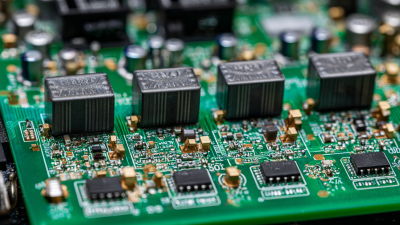
The Role of Automation in Enhancing PCB Assembly Efficiency
The role of automation in enhancing PCB assembly efficiency has become increasingly pivotal as the demand for faster, more complex designs continues to rise. With the growing adoption of advanced PCB design software powered by AI and innovative manufacturing processes, engineers are no longer bound by the traditional limitations of manual assembly. Automation technologies are redefining the landscape of PCB manufacturing, fostering the development of intricate circuit designs while streamlining production processes.
Moreover, the integration of smart manufacturing solutions is expected to propel the industry towards unprecedented efficiency levels. The push for automation, driven by Industry 4.0 trends, has led to significant advancements in automated PCB assembly methods, including enhanced pick-and-place machines and sophisticated defect detection systems. These innovations not only improve assembly speed but also increase quality assurance, allowing manufacturers to identify and address defects rapidly. As such, the marriage of automation and PCB assembly is set to revolutionize the electronics industry, facilitating a new era of precision and efficiency.

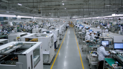
Best Practices for Streamlining Component Sourcing and Management
In today's competitive landscape, optimizing component sourcing and management is paramount for enhancing PCB manufacturing assembly efficiency. As the outsourced procurement market is projected to grow from $508.14 billion in 2024 to $1,050.94 billion by 2031, with a compound annual growth rate of 10.94%, manufacturers must prioritize effective sourcing strategies. Collaborating with reliable suppliers and leveraging data-driven insights can streamline operations, reduce lead times, and ensure that high-quality components are readily available.
Furthermore, integrating advanced supply chain management practices is essential for navigating the complexities of component management. By adopting a holistic approach that incorporates AI and smart optimization, manufacturers can enhance visibility and responsiveness across the supply chain. This not only facilitates better inventory management but also aligns sourcing decisions with production needs, ultimately driving a more efficient assembly process. The effective management of these components not only supports cost reduction but also fosters innovation, enabling companies to respond swiftly to market demands while maintaining high standards of quality.
Innovative Testing Methods to Improve PCB Quality and Reduce Waste
Innovative testing methods are crucial for enhancing PCB quality and reducing waste in the electronics manufacturing industry. The integration of AI-powered optical inspection (AOI) is revolutionizing the way we detect nanoscale defects in printed circuit boards. Recent studies indicate that AOI systems can identify issues related to soldering, connections, pads, and traces with remarkable accuracy, thus ensuring that only high-quality circuit boards reach the market. This advancement not only improves product reliability but also minimizes the costs associated with post-production failures, as defects can be caught early in the manufacturing process.
Moreover, the shift towards sustainable practices is driving the development of alternative materials for PCB substrates. Research on lignocellulose nanofibrils (LCNF) has unveiled their potential as eco-friendly substrates, which could significantly lower the environmental impact of PCB production. With the global electronics market projected to grow substantially, embracing sustainable innovations like LCNF could be a game-changer, offering a feasible path towards circular economy practices in the industry. These advancements place companies that adapt early in a competitive advantage, highlighting the necessity for ongoing investment in innovative manufacturing technologies.
5 Best Strategies for Optimizing PCB Manufacturing Assembly Efficiency - Innovative Testing Methods to Improve PCB Quality and Reduce Waste
| Strategy |
Description |
Expected Improvement (%) |
Implementation Time (Weeks) |
Estimated Cost ($) |
| Automated Inspection |
Implementing automated optical inspection (AOI) systems to detect defects early in the assembly line. |
20 |
6 |
15,000 |
| Lean Manufacturing |
Adopting lean principles to minimize waste and improve efficiency throughout the production process. |
15 |
8 |
8,000 |
| Data Analytics |
Using data analytics to monitor production metrics and identify bottlenecks in real time. |
25 |
12 |
10,000 |
| Quality Control Protocols |
Establishing strict quality control measures at multiple stages of assembly to ensure high standards. |
18 |
4 |
5,000 |
| Employee Training |
Regular training sessions for employees on new technologies and best practices in assembly processes. |
10 |
3 |
2,000 |
Implementing Lean Manufacturing Principles in PCB Assembly Processes
Implementing Lean Manufacturing Principles in PCB Assembly Processes can drastically enhance efficiency and reduce waste. Lean principles focus on streamlining processes, eliminating non-value-added activities, and improving overall workflow. One effective strategy is to map out the entire assembly process using Value Stream Mapping. This visual representation helps identify bottlenecks and areas of improvement, allowing teams to prioritize actions that enhance the assembly line flow.
Another crucial tip is to emphasize standardized work procedures. By establishing clear and consistent processes, teams can minimize variability and maintain quality. Training employees on these procedures ensures everyone is aligned and knowledgeable, reducing errors and increasing output. Additionally, regular reviews of these standards can help adapt to changes in technology and market demands.
Finally, fostering a culture of continuous improvement is essential. Encourage employees to voice their ideas and suggestions for process enhancements. Implementing programs like Kaizen can motivate teams to focus on small, incremental changes that contribute to greater efficiency over time. Engaging the workforce in this way not only boosts morale but also drives innovation in the PCB assembly process.