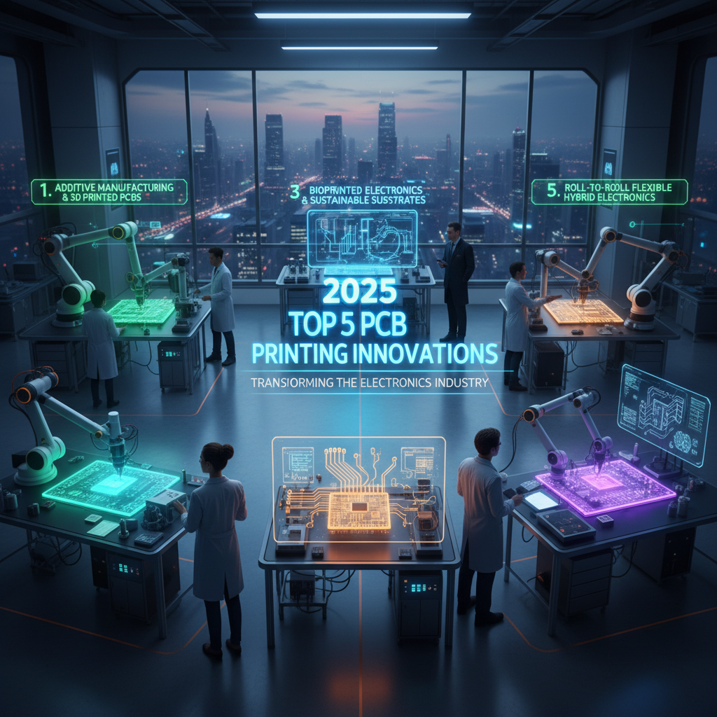
2025 Top 5 PCB Printing Innovations Transforming the Electronics Industry
As the electronics industry continues to evolve, the role of
PCB printing has become increasingly critical in driving
innovation and efficiency. According to a recent report by
Research and Markets, the global PCB market is projected to reach $100 billion by 2025,
with advancements in PCB printing technology playing a pivotal role in this growth. The emergence of new materials,
processes, and designs is reshaping the landscape, enabling manufacturers to meet the escalating demands for
higher functionality, miniaturization, and sustainability in electronic devices.
Dr. Emily Zhang, a leading expert in PCB technology, emphasizes the importance of these innovations:
"The future of electronics hinges on our ability to adapt and refine PCB printing techniques.
The integration of additive manufacturing and
smart materials will not only enhance product performance
but also reduce waste and production costs."
As we look ahead, five distinctive innovations in PCB printing are set to revolutionize the industry,
streamlining production and empowering engineers to push the boundaries of design capabilities, ultimately transforming
how we interact with electronic devices.
Emerging Techniques in PCB Printing: The Rise of 3D Printing Technologies
The rise of 3D printing technologies is revolutionizing the electronics manufacturing landscape, with innovations set to reshape the industry by 2025. Among these, 3D-printed electronics stand out for their potential to create functional components rapidly and at lower costs. As manufacturers increasingly adopt these techniques, the market for 3D-printed electronics is expected to expand significantly, paving the way for innovative practices and designs that were previously unattainable with traditional methods.
Moreover, the eco-friendly aspect of 3D-printed electronics cannot be overlooked. Emerging technologies are enabling the production of electronic devices that can dissolve in water, offering a sustainable solution for recycling and prototype creation. This innovation not only simplifies the recycling process but also aligns with growing environmental concerns, as it reduces electronic waste.
As the printed electronics devices market is projected to reach USD 62.9 billion by 2035, the integration of 3D printing is a fundamental aspect of this growth, further underlining its transformative potential within the electronics industry.
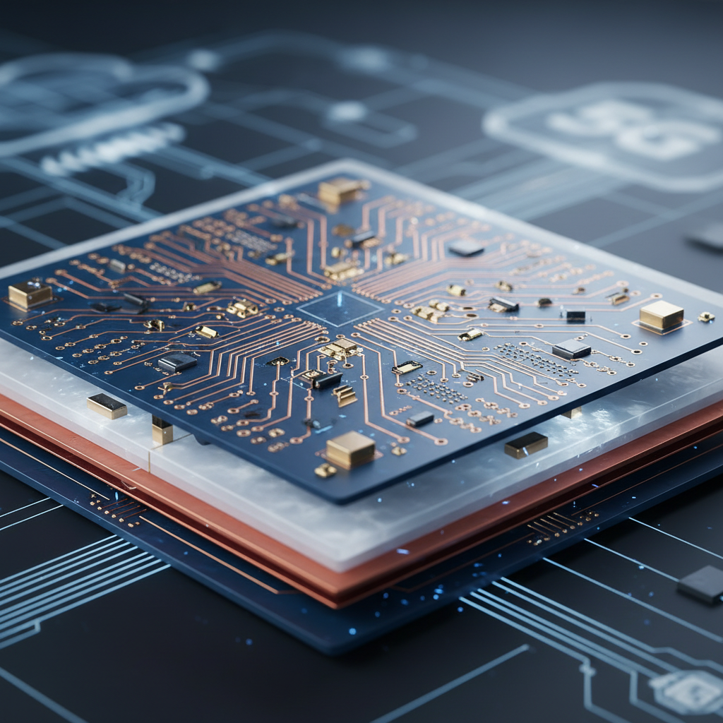
Advancements in Materials: The Shift Towards Flexible and Eco-friendly PCBs
The electronics industry is experiencing a revolutionary shift towards flexible and eco-friendly printed circuit boards (PCBs), driven by advancements in materials technology. According to a report by MarketsandMarkets, the global flexible PCB market is projected to grow from $24.4 billion in 2020 to $46.4 billion by 2025, reflecting a compound annual growth rate (CAGR) of 14.4%. This surge is attributed to the increasing demand for lightweight and compact electronic devices in sectors such as consumer electronics, automotive, and medical technology.
The push for eco-friendly PCBs is also gaining momentum, with industry leaders focusing on sustainable materials and processes to reduce the environmental impact of electronic waste. A study by the International Journal of Environmental Research and Public Health highlights that traditional PCBs often contain hazardous materials, but the development of biocompatible and recyclable materials is paving the way for greener alternatives. Companies are now experimenting with biodegradable substrates and non-toxic inks, which not only enhance the sustainability of PCB manufacturing but also meet the stringent regulatory requirements for environmental protection. This dual focus on flexibility and eco-friendliness is set to redefine the standards in the electronics manufacturing landscape.
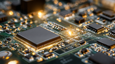
Integration of AI and Automation in PCB Manufacturing Processes
The integration of AI and automation in PCB manufacturing processes is reshaping the landscape of the electronics industry. By implementing advanced AI functionalities, manufacturers are enhancing their Electronic Design Automation (EDA) tools, significantly improving productivity and innovation. This transformation allows for faster design processes and streamlined workflows, enabling designers to bring their ideas to market more rapidly. The growth in the EDA sector underscores the importance of these innovations, as reflected in a projected market value increase from $31.7 billion in 2023 to $107.7 billion by 2032.
Moreover, the rise of off-line PCB laser depaneling systems highlights the trend towards automation and precision in manufacturing. With the market expected to grow from $141.41 million in 2024 to $203.26 million in 2032, this technology plays a crucial role in optimizing production efficiency and reducing costs. As the industry embraces AI-driven solutions, the potential for further advancements in PCB design and manufacturing processes becomes an exciting prospect for companies aiming to stay competitive in the ever-evolving electronics market.
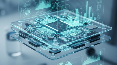
Enhancing Signal Integrity: Innovations in High-Frequency PCB Designs
The electronics industry is on the brink of a transformation, particularly through advancements in high-frequency PCB designs aimed at enhancing signal integrity. As more devices demand higher speeds and greater bandwidth, innovative techniques such as advanced material selection and optimized layouts are being implemented. These innovations enable PCs and other electronic devices to maintain performance metrics vital for applications like cloud computing and 5G telecommunications.
Additionally, the emergence of high-speed interconnects further emphasizes the critical nature of efficient PCB designs in modern infrastructures. With the market for high-speed interconnects projected to reach $56.9 million by 2030, driven by the rising demands from data centers and AI/ML technologies, manufacturers must prioritize research and development to remain competitive. Continuous investment in cutting-edge solutions not only enhances the functionality of PCBs but also positions companies to capitalize on the rapidly evolving technological landscape.
Cost Reduction Strategies: The Role of Rapid Prototyping in PCB Production
The push for cost reduction in PCB production is driving significant innovations in rapid prototyping. Companies are increasingly investing in advanced technologies like fiber lasers to enhance efficiency and reduce manufacturing costs. Chittaranjan Behera from JC Eletronica noted that their recent patent successes highlight the potential of these technologies to revolutionize PCB manufacturing. Such advancements not only streamline production but also enable faster turnaround times, crucial for businesses looking to remain competitive.
Tips: Embrace rapid prototyping to drastically lower development costs and test new designs efficiently. Implementing technologies such as fiber lasers can yield high precision while minimizing material waste.
Another notable innovation comes from Salgenx, which is developing a low-cost method for circuit board production using graphene and hard carbon-coated materials. This approach promises to deliver enhanced performance at a fraction of the traditional cost, underscoring the importance of sustainable practices in the electronics industry.
Tips: Keep an eye on emerging materials like graphene that offer both performance benefits and cost efficiency. Investing in research and development can lead to breakthroughs that transform production processes.
2025 Top 5 PCB Printing Innovations Transforming the Electronics Industry
This chart illustrates the projected cost reduction achieved through different PCB printing innovations, emphasizing the role of rapid prototyping in PCB production.